logo
Datasheet4U.com - NCV8186
logo

NCV8186 Datasheet, Regulator, ON Semiconductor

NCV8186 Datasheet, Regulator, ON Semiconductor

NCV8186

datasheet Download (Size : 423.24KB)

NCV8186 Datasheet
NCV8186

datasheet Download (Size : 423.24KB)

NCV8186 Datasheet

NCV8186 Features and benefits

NCV8186 Features and benefits


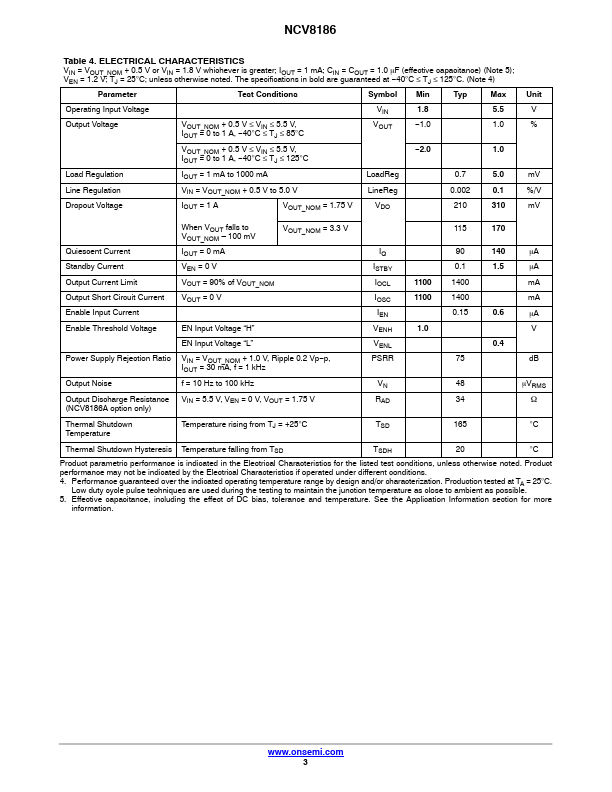
* Operating Input Voltage Range: 1.8 V to 5.5 V
* Output Voltage Range: 1.2 to 3.9 V
* Quiescent Current typ. 90 mA
* Low Dropout: 100 mV typ. at 1 A, VOU.

NCV8186 Application

NCV8186 Application

Requiring Unique Site and Control Change Requirements; AEC−Q100 Qualified and PPAP Capable
* These Devices are Pb−Fr.
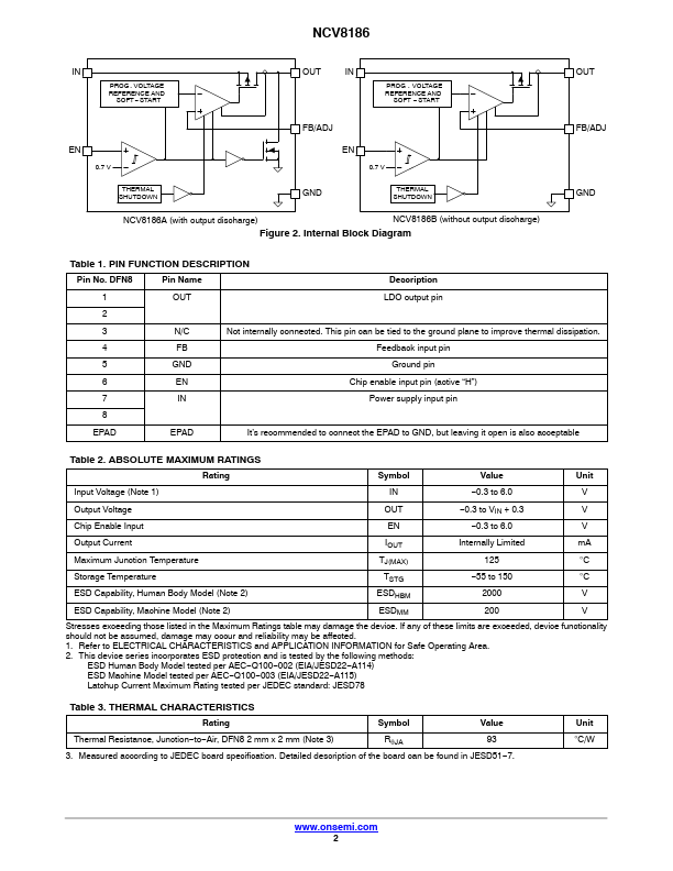
NCV8186 Description

NCV8186 Description

Pin No. DFN8 Pin Name Description 1 OUT LDO output pin 2 3 N/C Not internally connected. This pin can be tied to the ground plane to improve thermal dissipation. 4 FB Feedback input pin 5 GND Ground pin 6 EN Chip enable input pin (.

Image gallery

NCV8186 Page 1 NCV8186 Page 2 NCV8186 Page 3

TAGS

NCV8186
Fast
Transient
Response
Low
Voltage
LDO
Regulator
ON Semiconductor

Manufacturer


ON Semiconductor (https://www.onsemi.com/)

Related datasheet

NCV8184

NCV8187

NCV8189

NCV81071

NCV8114

NCV8130

NCV8133

NCV81341

NCV81341P

NCV8135

NCV8141

NCV8154

NCV81599

Since 2006. D4U Semicon.   |   Datasheet4U.com   |   Contact Us   |   Privacy Policy   |   Purchase of parts